Photonic Computing: A Light-Based Architectural Response to the End of Electronic Scaling
Abstract
Artificial intelligence workloads now routinely exceed 100 trillion parameters [23], yet the copper interconnects that move data between processors and the silicon transistors that compute on it are simultaneously approaching their fundamental electrical limits. This paper argues that photonic computing, a paradigm that combines light-based on-chip and off-chip interconnects with multi-level frequency and wavelength encoding, represents the most credible architectural response to the end of Moore's Law scaling and the bandwidth and power crisis of the artificial intelligence era. The argument proceeds in seven sections: a historical arc from mechanical calculation to the present, a technical case for photonic advantage, a survey of quantitative benchmarks, a risk analysis covering manufacturing and accuracy tradeoffs, a commercialization forecast, a comparison with rival paradigms, and a policy conclusion. The paper presents both the verified benefits and the verified risks of the technology. The position it defends is aggressive hybrid electronic-photonic deployment now, with all-optical maturation targeted over the coming decade.
1. Introduction
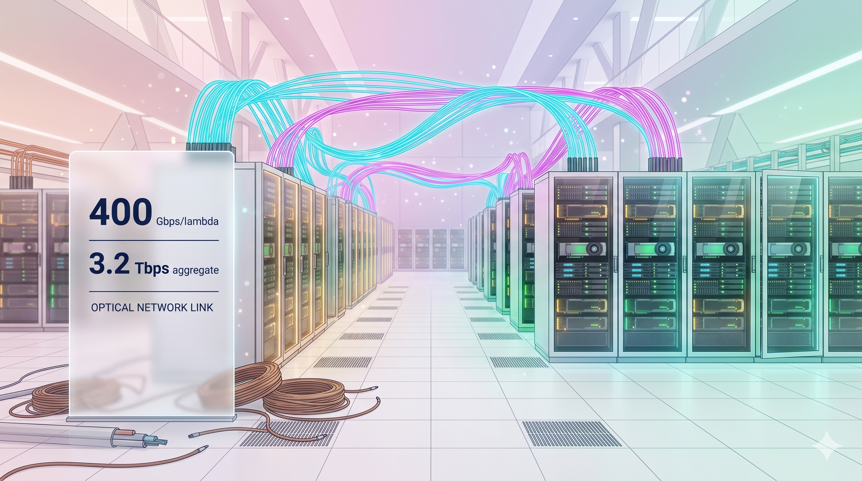
Modern large language models have crossed the 100 trillion parameter threshold [23], and the data centers training them pack 8 to 16 GPUs per NVIDIA DGX node communicating over 900 GB/s internal links and 400 Gb/s InfiniBand channels between nodes [23]. Every one of those channels still carries its signal as electrons through copper. Copper, however, is running out of room. The power consumed per unit of bandwidth in electrical interconnects has improved by more than 30 times over the past 20 years [6], yet that curve is visibly flattening, and the resistance-capacitance product (commonly called RC delay, the time constant that governs how fast a signal can charge or discharge a wire) grows with integration density rather than shrinking. At the same time, silicon photonic transceivers have pushed single-wavelength bandwidth to 400 Gbps and aggregate throughput to 3.2 Tbps across eight channels on a single chip [11]. A physical gap has opened between what the workloads demand and what the wires can deliver.
This paper argues that photonic computing, defined for the purposes of this paper as any computing architecture that encodes and processes information primarily in optical degrees of freedom, namely wavelength, frequency, phase, polarization, and spatial mode, is the most credible architectural response to that gap. The thesis has three parts. First, the electronic scaling trends that powered the last 60 years of progress have broken in ways that additional transistor-level engineering cannot fix. Second, decades of parallel development in optical communications have produced a mature toolkit of components, including silicon waveguides (the on-chip equivalent of optical fiber), wavelength-division multiplexing (WDM) transmitters, and integrated modulators, that is now ready to move from the data center backbone onto the processor die itself. Third, combining these optical interconnects with emerging frequency-encoded logic and multi-dimensional photonic computing yields performance and energy figures that no electronic roadmap currently matches.
The rest of the paper is organized as follows. Section 2 traces the history of computing technology from mechanical calculation through transistors, integrated circuits, and the breakdown of Dennard scaling, and then follows a parallel optical timeline from the 1970 wavelength-division multiplexing concept to modern silicon photonics. Section 3 presents the core technical case for light-based computation. Section 4 surveys quantitative performance and energy benchmarks. Section 5 addresses the honest risks: manufacturing complexity, accuracy gaps on some classification tasks, photon loss, and the still-imperfect opto-electronic interface. Section 6 reviews commercialization. Section 7 concludes with a policy recommendation.
The step-back framing that guides the paper is this: computation is not a free abstract operation. It consumes physical resources, specifically electrons moved through wires, heat dissipated through packages, and time spent waiting for signals to arrive. When we ask why photonic computing matters, the answer is that the electron-centric version of those three resources is becoming constrained all at once, and only a change of physical carrier can relieve all three constraints together.
2. A Short History of Computing Technology and the Road to Photonics
2.1 From mechanical calculation to the vacuum tube
The historical arc that leads to photonic computing begins long before the chip. Charles Babbage's Analytical Engine, designed in the 1830s, encoded arithmetic in the angular position of brass gears. Herman Hollerith's tabulating machines mechanized the 1890 United States census by passing electrical probes through punched cards. A century later, the ENIAC used roughly 17,000 vacuum tubes to represent binary state in the on or off conduction of a heated filament. Each step changed the physical carrier of information, first gears, then card holes and relays, then free electrons in a vacuum, and each step delivered a roughly order-of-magnitude gain in speed over the previous one. The pattern is worth naming: every major computing era has corresponded to a change in the physical medium that carries a bit.
Every major computing era has corresponded to a change in the physical medium that carries a bit. The question is not whether photons follow electrons; it is when.
Historical framing, Section 2.1
2.2 The transistor and the integrated circuit
The transistor, invented at Bell Labs in 1947, replaced the vacuum tube with a solid-state switch built from doped semiconductors. Because a transistor has no filament to heat, it consumed dramatically less power and could be made dramatically smaller. The integrated circuit, demonstrated independently by Jack Kilby at Texas Instruments and Robert Noyce at Fairchild Semiconductor in the late 1950s, then collapsed many transistors onto a single slab of silicon. From that point onward, computing performance was governed by how many transistors engineers could cram into a given area.
2.3 Moore's Law and Dennard scaling
Gordon Moore's 1965 observation, later sharpened into the rule that transistor counts double roughly every two years [8], described the geometric side of that cramming. The companion rule, formulated by Robert Dennard at IBM in 1974, described the electrical side: as transistor dimensions shrank, voltage and current could shrink with them, keeping power density roughly constant. Together, Moore's Law and Dennard scaling gave the industry a four-decade run in which clock frequencies, transistor counts, and energy efficiency all improved simultaneously, and complementary metal oxide semiconductor (CMOS) technology rode the curve.
2.4 The breakdown of Dennard scaling and the rise of specialization
Around 2005 the Dennard half of the bargain collapsed. As transistors shrank below roughly 90 nanometers, leakage currents and heat density refused to cooperate, and clock frequencies stalled near 3 to 4 GHz. The industry responded not with faster cores but with more of them, and then with specialized accelerators. Graphics processing units (GPUs), originally built for rendering triangles, became the workhorse of deep learning. Application-specific integrated circuits (ASICs) such as Google's Tensor Processing Unit (TPU) pushed that specialization further, trading generality for throughput on matrix-multiplication-heavy workloads. Specialization bought the industry another decade, but it did not solve the underlying physical problem.
2.5 The bandwidth and power wall
The wall that specialization ran into is built of two bricks. The first is RC delay: the product of wire resistance (R) and wire capacitance (C) that sets how fast an electrical signal can be driven through a copper interconnect. As wires scale down in width, their resistance rises faster than their capacitance falls, so RC delay gets worse, not better, at each new process node. The second brick is energy per bit. Marvell reports that silicon photonic transceivers have cut power consumption per unit bandwidth by more than 30 times over the last 20 years, pushed bandwidth density per unit volume up 10 times, and increased bandwidth per module by 400 times [6], but the electrical side of the same link has seen much more modest gains and is visibly flattening. When an NVIDIA DGX node needs 900 GB/s of internal bandwidth and 400 Gb/s of external bandwidth per GPU simply to keep its cores fed [23], every picojoule per bit matters.
2.6 The parallel optical timeline
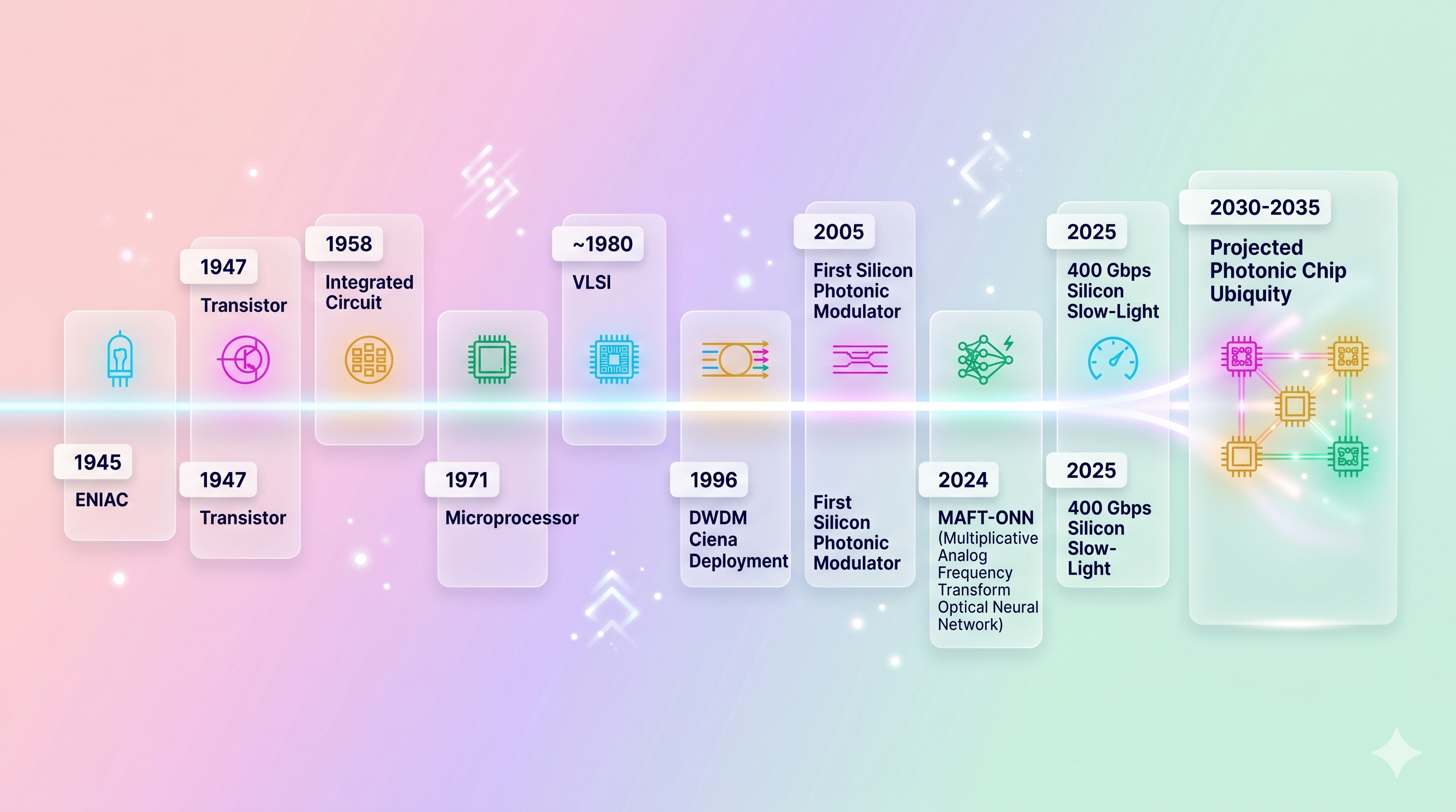
While electronic scaling was peaking and then stalling, optical communications went through its own multi-decade buildout. The concept of wavelength-division multiplexing, that is, sending several independent data streams down the same fiber on different colors of light, was first published in 1970 by O. E. Delange in the Proceedings of the IEEE [21]. W. J. Tomlinson and C. Lin demonstrated an optical wavelength-division multiplexer covering the 1 to 1.4 micrometer spectral region in 1978 [21]. H. Ishio, J. Minowa, and K. Nosu reviewed the field in 1984 in the Journal of Lightwave Technology [21], and laboratory WDM systems were operational by 1980 [21].
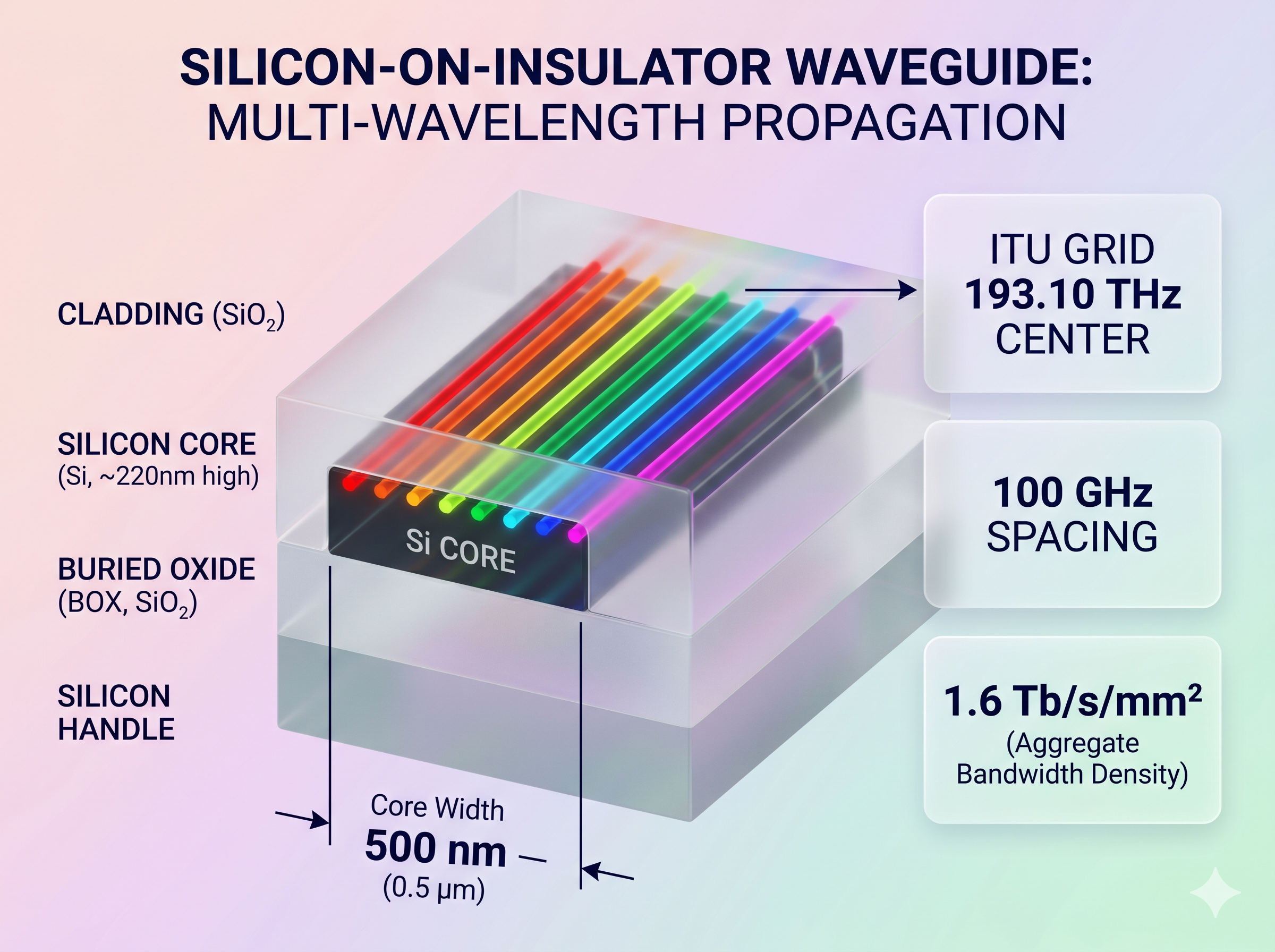
The 1990s turned the laboratory work into commercial infrastructure. Ciena deployed the first commercial dense wavelength-division multiplexing (DWDM) system on the Sprint network in June 1996 [21]. IBM's Muxmaster, reported in 1997, transmitted 20 wavelengths at up to 2 Gbit/s each over a single fiber [18]. The International Telecommunication Union standardized the DWDM frequency grid (ITU-T G.694.1) with a reference frequency of 193.10 THz, equivalent to a wavelength of 1552.52 nm [21], and proposed 100 GHz spacing, roughly 0.8 nm between channels, in 1997 [18]. By the 2020s, commercial DWDM systems commonly carry 40 channels at 100 GHz spacing or 80 channels at 50 GHz spacing, and 160-signal systems push aggregate capacity past 16 Tbit/s on a single fiber [21]. A 320-channel system with 12.5 GHz channel spacing has been demonstrated [21]. Critically, the toolkit built for long-haul telecommunications (tunable lasers, Mach-Zehnder modulators, erbium-doped fiber amplifiers, arrayed waveguide gratings) is the same toolkit now being shrunk onto silicon photonic chips.
2.7 Early all-optical logic and frequency encoding
The telecommunications track gave photonics its bandwidth. A second, quieter research track gave it the first proposals for computing with light directly. S. K. Garai's 2011 Applied Optics paper demonstrated all-optical frequency-encoded conversion between decimal, binary-coded decimal, and Gray code using semiconductor optical amplifiers [5]. S. Dutta and S. Mukhopadhyay published an alternating approach to frequency-encoded all-optical logic gates in Optik the same year [10]. On the quantum side, J. M. Lukens and P. Lougovski's 2016 Optica paper laid the theoretical foundation for frequency-encoded photonic qubits as a scalable substrate for quantum information processing [15], and Oak Ridge National Laboratory launched a matching experimental project under N. A. Peters in October 2016 [16]. These efforts established that frequency, the specific oscillation rate of a light wave, is a usable logical and quantum degree of freedom in its own right, not merely a channel label for classical traffic.
2.8 Convergence
The three tracks, electronic scaling hitting a wall, silicon photonics maturing as a manufacturable platform, and frequency-encoded logic moving from theory into the laboratory, are now converging. Artificial intelligence workloads supply the demand. Silicon photonic transceivers, now capable of 400 Gbps per wavelength and 1.6 Tb/s/mm2 on-chip density [11], supply the interconnect. Multi-dimensional photonic computing architectures have demonstrated more than 217 tera-operations per second on diffractive optics and more than 11 TOPS using combined time, wavelength, and spatial multiplexing, with energy efficiencies up to three orders of magnitude better than traditional chips [7]. The MIT Multiplicative Analog Frequency Transform Optical Neural Network (MAFT-ONN), a three-layer optical deep neural network, computes more than four million fully analog operations per inference using photoelectric multiplication between radio-frequency-encoded optical frequency combs [17]. The convergence point is the thesis of this paper: the physical carrier of computation is ready to change again, this time from the electron to the photon.
3. The Physical Basis of Photonic Computing Advantages
3.1 Why Light? The Physics of Signal Transport
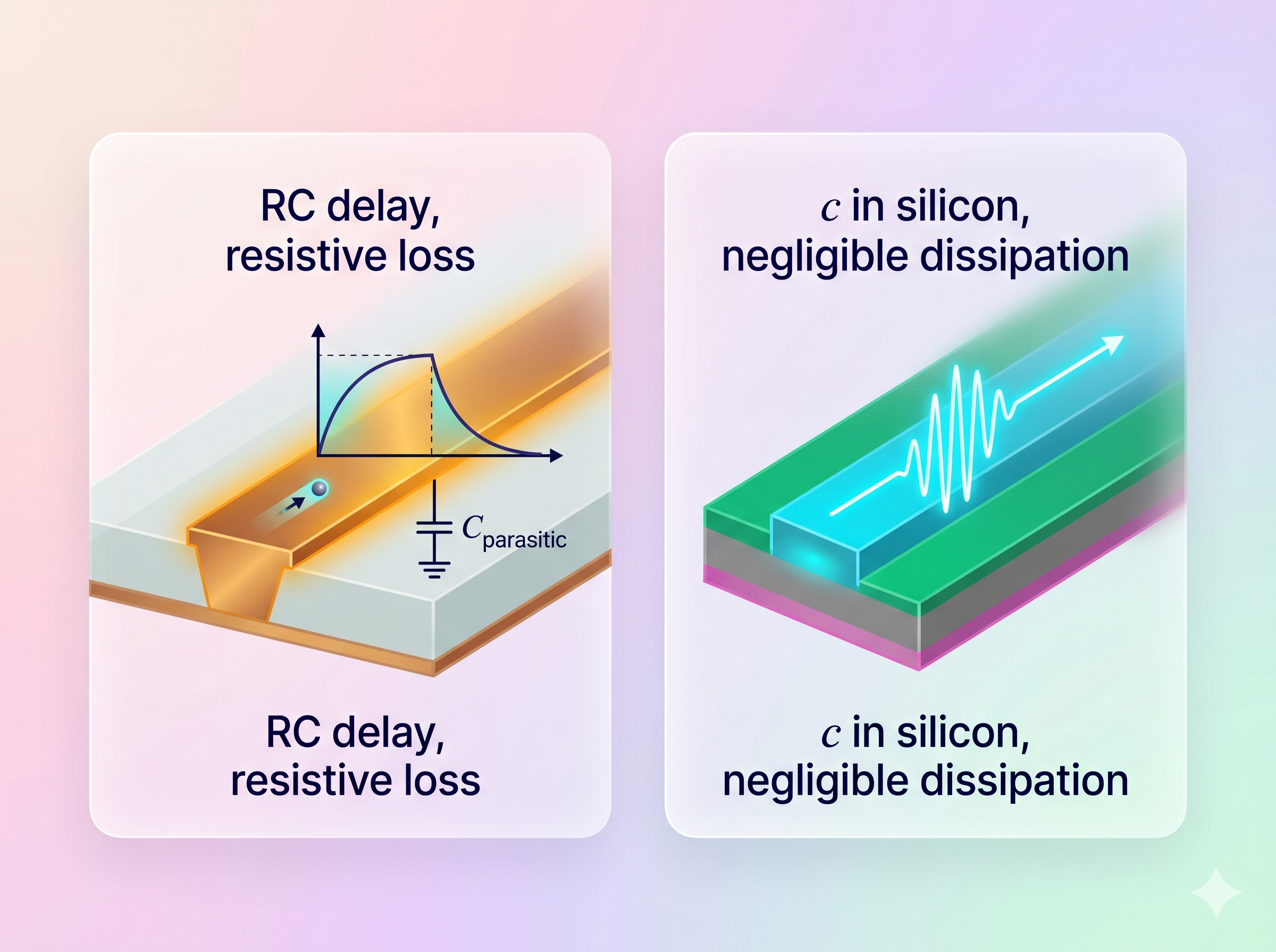
Every electronic interconnect on a conventional chip behaves like a tiny capacitor that must be charged and discharged to transmit a single bit. The time constant governing this process, commonly called RC delay (the product of the wire's resistance R and its capacitance C), grows as transistors shrink and wires become thinner and more densely packed [1], [4]. Shrinking a wire cross-section raises its resistance, while packing wires closer together raises their mutual capacitance, so the delay does not simply scale down with feature size. As chip clock rates climbed into the gigahertz range, copper interconnects became a dominant bottleneck for both latency and power, a limitation that the University of Arizona's photonic computing group identifies as one of the central motivations for switching carriers [4].
Photons carry information through a fundamentally different mechanism: they propagate as electromagnetic waves and do not charge any capacitance along the way. There is no RC time constant on a photonic channel because no charge is being moved from one plate to another. Instead, signals travel through waveguides, which are narrow channels (typically a few hundred nanometers wide for silicon photonics) etched into a silicon substrate that confine light by total internal reflection, analogous to how fiber-optic cables guide light over long distances. In vacuum, light travels at roughly 300 million meters per second [3]. Inside silicon, photons move at c divided by the refractive index n, where n is approximately 3.5 for silicon at telecom wavelengths [8], giving a propagation speed near 86 million meters per second. This is still orders of magnitude faster than electrical signal propagation through the RC-limited copper meshes of modern processors, and Dudhia's analysis records full light traversal through a nanophotonic neural-network circuit in only 31 picoseconds [8].
The energy consequence is equally important. Because no capacitor is being charged at every toggle, the per-bit energy cost of moving information collapses. Depletion-mode resonant silicon modulators already reach 1 femtojoule per bit at 25 gigabits per second [23], and sub-picojoule targets are within reach. Critically, silicon photonics inherits the manufacturing infrastructure of mainstream microelectronics. As Han et al. put it, "silicon photonics is an important platform with high complementary metal-oxide semiconductor (CMOS) compatibility, which brings the feasibility of low-cost and large-scale production" [11], where CMOS refers to the standard silicon fabrication process used for essentially all modern microprocessors. The physics favors photons, and the fabrication economics do not punish the switch.
3.2 Wavelength-Division Multiplexing (WDM): Parallelism Built Into Physics
Wavelength-division multiplexing, or WDM, is the technique of sending many independent data streams down a single optical channel by assigning each stream a different wavelength (color) of light. Because photons of different wavelengths do not interact linearly with one another, two or more signals can share one waveguide without mutual interference, a form of parallelism that is simply not available to electrons sharing a copper wire. The concept was first published by O. E. Delange in 1970 in the Proceedings of the IEEE, laboratory WDM systems were operational by 1980, and dense WDM (DWDM) entered commercial deployment in June 1996 on the Sprint network via Ciena [21].
Modern systems exploit this parallelism at enormous scale. Typical DWDM installations carry 40 channels at 100 gigahertz spacing or 80 channels at 50 gigahertz spacing, and 160-signal deployments push aggregate capacity past 16 terabits per second over a single fiber [21]. Extreme configurations have demonstrated 320 channels at 12.5 gigahertz spacing [21]. The standard DWDM windows are the C-band (1530 to 1565 nanometers) and the L-band (1565 to 1625 nanometers) [21], both chosen because erbium-doped fiber amplifiers work efficiently there. The same principle scales down to the chip. Han et al. reported an 8-channel silicon photonic system with 3.2 terabits per second aggregate throughput and 1.6 terabits per second per square millimeter on-chip density [11]. Commercial efforts push further still: Xscape Photonics, a Columbia University spinout founded by Gaeta, Lipson, Bergman, Raghunathan, and Okawachi, builds multi-wavelength programmable laser platforms where a single source generates "hundreds of different colors of light" to drive data-center fabrics [12].
The analytical takeaway is that WDM turns the optical medium itself into a natural parallel bus. An electronic system must spend silicon area and energy to build additional physical lanes; a photonic system exploits the wavelength dimension, which is essentially free once the lasers and filters are in place.
3.3 Multi-Level Encoding: Beyond Binary
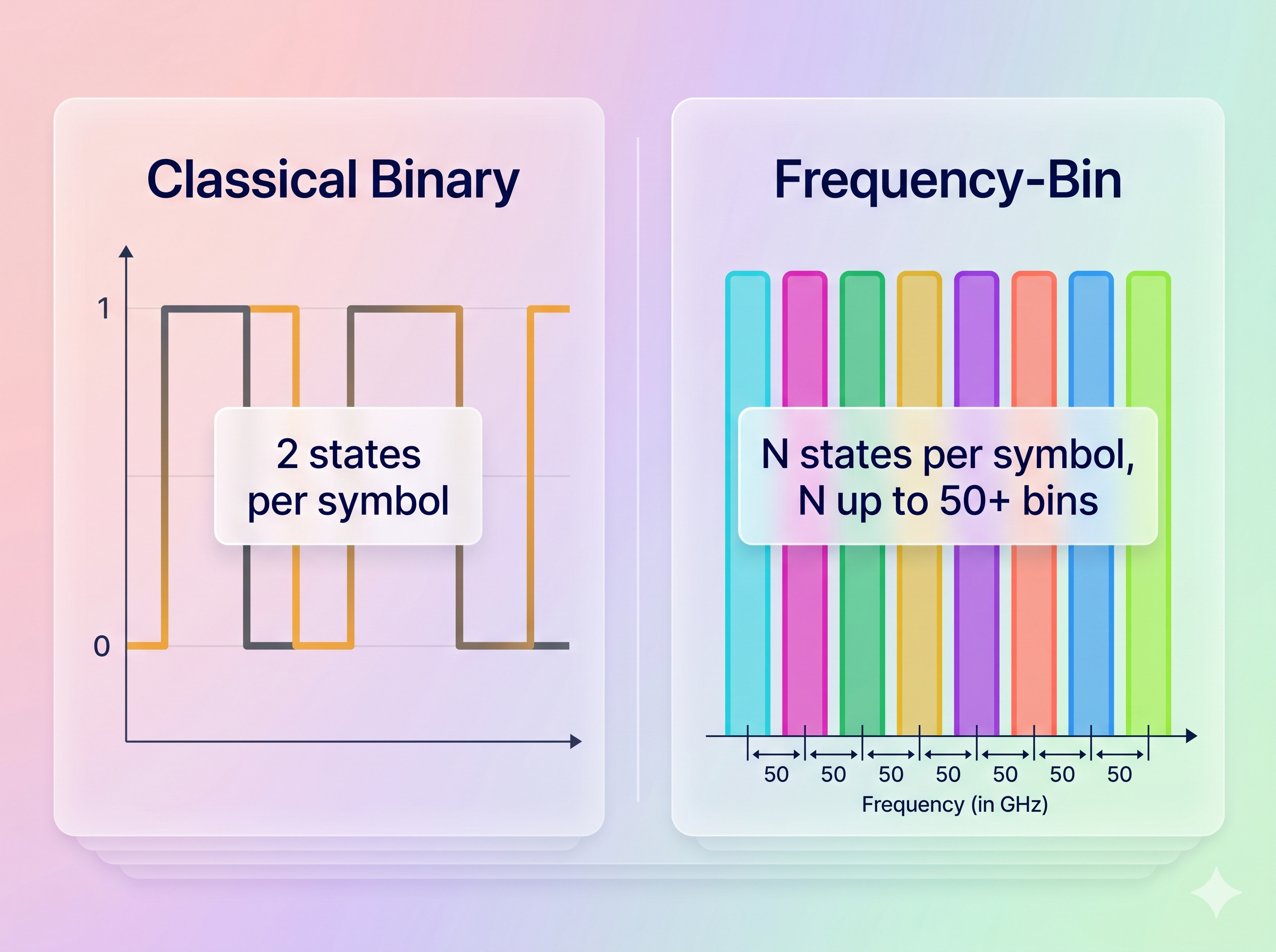
Electronic digital logic encodes information in binary, meaning each signal takes only one of two discrete voltage levels (conventionally 0 and 1). Optics offers richer alphabets. The intuitive picture is a signal that chooses among eight distinct colors labeled A through H: a single photon of the right frequency carries three bits of information at once, rather than just one. Two complementary families of multi-level schemes are already demonstrated in hardware.
The first family encodes multiple levels into the amplitude of a signal. Pulse-amplitude modulation with four levels, PAM-4, is the IEEE standard behind 224 gigabit-per-second optical transceivers [11]. PAM-8, which uses eight distinguishable amplitude levels, pushed a single silicon slow-light modulator to 390 gigabits per second in the Han et al. demonstration [11]. The second family encodes information directly into the frequency (or color) of the photon. Garai's 2011 work on all-optical frequency-encoded decimal-to-binary converters using semiconductor optical amplifiers [5] and Dutta and Mukhopadhyay's 2011 frequency-encoded all-optical logic gates and flip-flops [10] laid the groundwork by showing that the frequency of a photon is preserved under reflection, refraction, and absorption, giving encoded data intrinsic robustness. Lukens and Lougovski's 2016 paper is widely cited as the foundational proposal for spectral linear-optical quantum computation, in which qubits are encoded in discrete frequency bins and processed with electro-optic modulators and pulse shapers [15]. Oak Ridge National Laboratory's Peters project, started in October 2016, builds matter-qubit interconnects using electro-optic frequency beam splitters and "tritters" (three-way frequency-mode mixers) [16]. A 2024 free-space feasibility study by Vinet et al. achieved frequency-bin spacings up to 50 gigahertz with electro-optic modulators, operated at 780 nanometers, and reported Z-basis visibility of 85.5 plus or minus 2.2 percent and X-basis visibility of 92.4 plus or minus 2.7 percent for photonic qubits crossing a 2-meter free-space link [24]. On the classical side, Pintus et al. demonstrated multi-level magneto-optic memory cells using cerium-substituted yttrium iron garnet on silicon micro-ring resonators with 2.4 billion switching cycles, three orders of magnitude better endurance than competing non-volatile approaches [22]. A resonator here is a small ring-shaped waveguide that traps light at specific wavelengths.
Multi-level encoding multiplies the information content of every photon, directly attacking the bottleneck that binary electronics cannot escape: a silicon transistor has only two stable states, but a photon has a continuum.
3.4 Native Parallelism in Linear Algebra
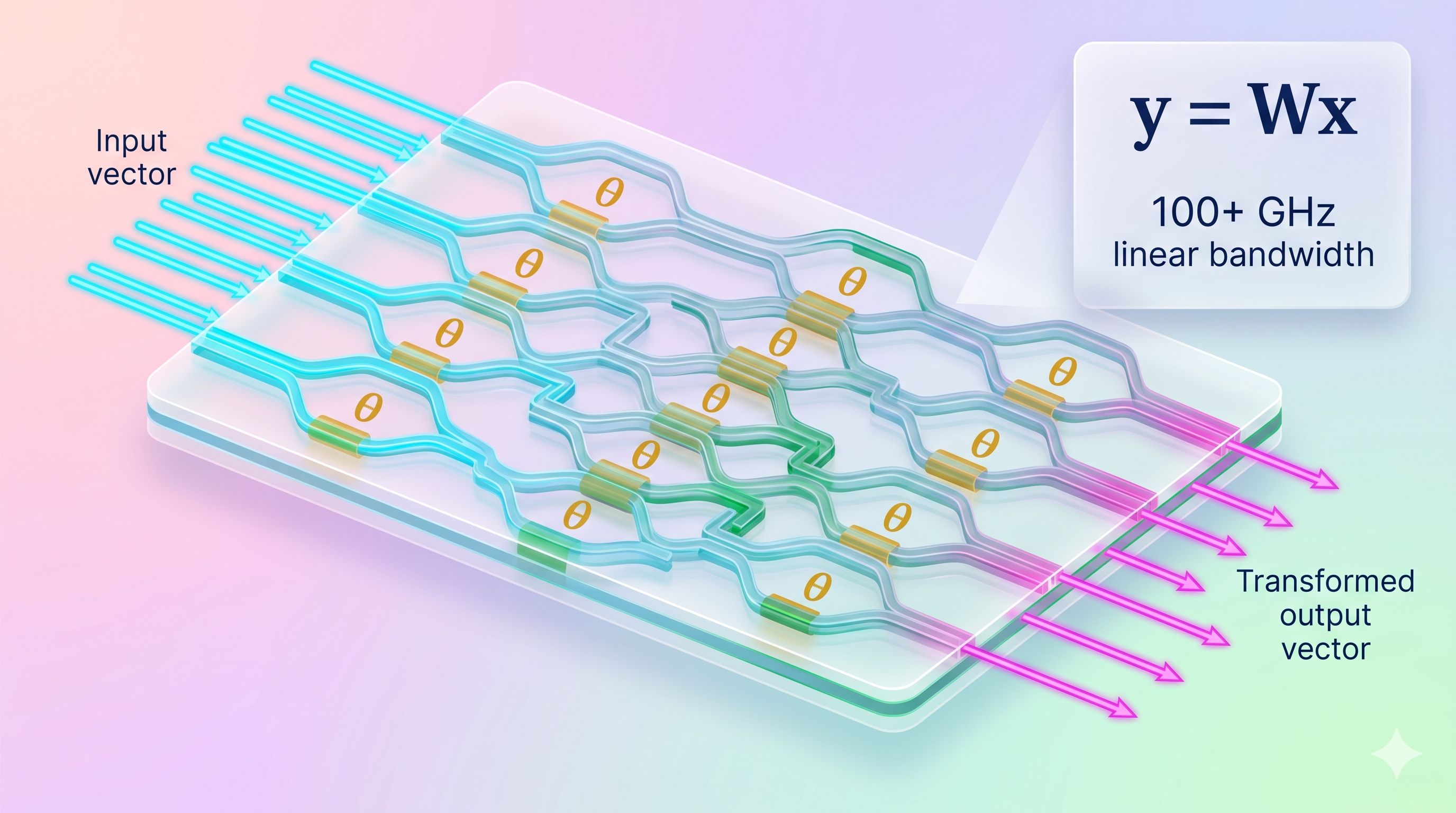
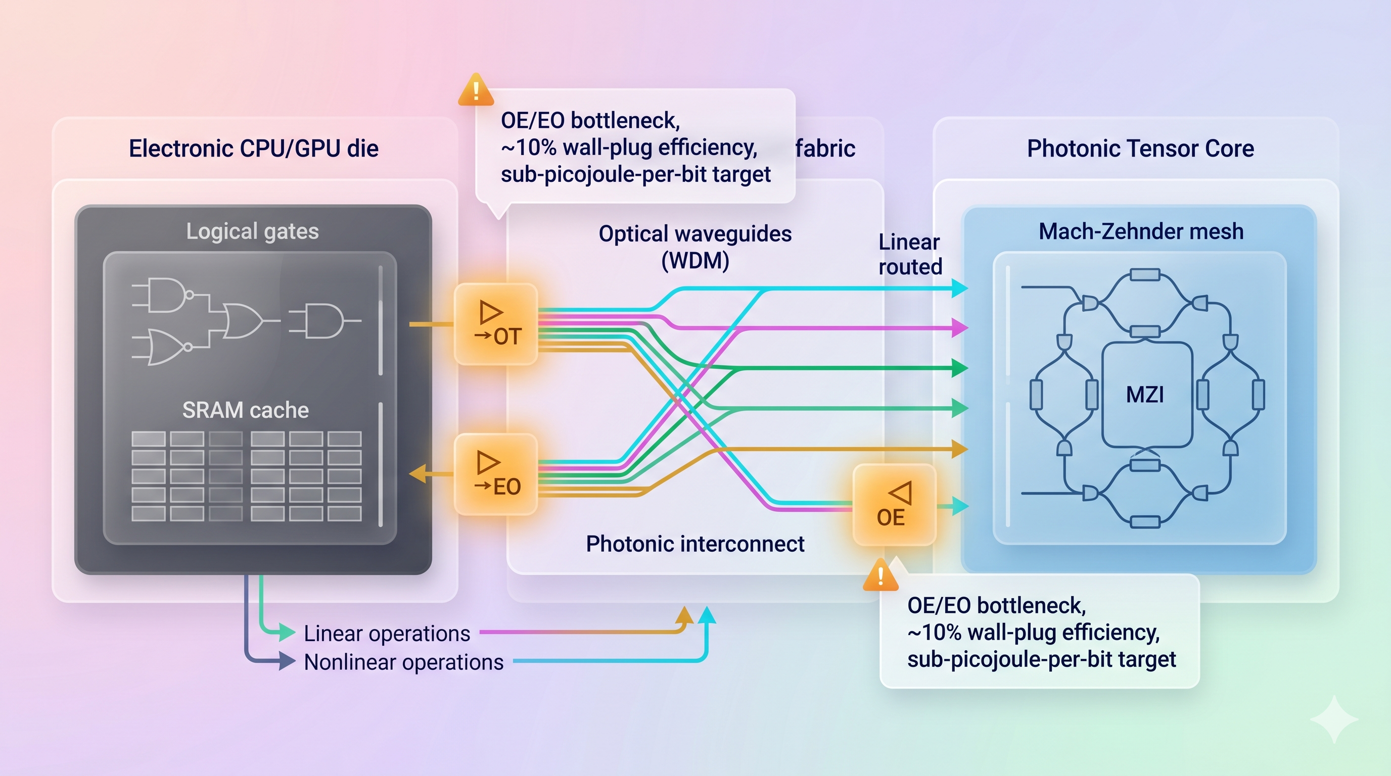
The dominant computation inside modern deep-learning hardware is matrix-vector multiplication, the operation that sits at the core of every convolution, transformer attention layer, and fully connected layer. A tensor core, the specialized unit in an NVIDIA GPU, accelerates this operation by sequencing billions of multiply-accumulate steps in parallel across thousands of transistors. Photonic computing takes a different route: matrix-vector multiplication can be made to happen physically, in a single pass of light through a programmable mesh of waveguides and interferometers, without sequencing any electronic multiplications at all.
The mapping is direct. A mesh of Mach-Zehnder interferometers (pairs of waveguides that split and recombine light with programmable phase shifts) can be configured so that light entering with an input vector emerges carrying the product of that vector and a matrix encoded in the phase settings. Guo et al. formalized this approach in a photonic general matrix-matrix multiplication (GEMM) accelerator published in IEEE JSTQE in 2022 [19]. MIT's MAFT-ONN architecture, invented by Dirk Englund and Ronald Davis, uses radio-frequency-encoded optical frequency combs (combs are laser outputs with many equally spaced spectral lines) to perform photoelectric multiplication, and its three-layer deep neural network "can compute over four million fully analog operations" in a single shot [17]. Dudhia measured linear transformations inside optical neural networks running at more than 100 gigahertz [8], and Swayne's report on the 2025 Nature Reviews Physics study catalogued 217 tera-operations per second (TOPS) on a diffractive-optics chip and more than 11 TOPS on a system combining time, wavelength, and spatial multiplexing, with energy efficiencies up to three orders of magnitude better than traditional chips [7]. Dudhia's benchmarking sharpens the comparison: a photonic image classifier completes inference in 570 picoseconds using 2.1375 nanojoules, versus 153,580 joules on a classical GPU baseline for the same workload [8], a roughly seventy-trillion-fold energy gap.
The deeper reason is structural. A photonic tensor core performs the matrix operation as a physical linear optical transformation, not as a sequenced computation. Light enters, interferes, and exits, and the answer is available at the output detectors within a single traversal of the chip. Nothing is "clocked." The parallelism is not built from transistors; it is built from the Maxwell equations.
The parallelism is not built from transistors. It is built from the Maxwell equations.
Section 3.4, Native parallelism in linear algebra
4. Empirical State of Photonic Computing
4.1 Laboratory Performance Benchmarks
Peer-reviewed laboratory demonstrations over the past two years establish that photonic computing has crossed the threshold from theoretical promise into measured performance. Han et al., publishing in Nature Communications in July 2025, reported silicon slow-light modulators (optical devices that delay light to increase its interaction time with an electrical signal, improving modulation efficiency) operating at 400 Gbps per wavelength with a 90 GHz electro-optic bandwidth, a modulation efficiency of 0.82 V*cm, and a static extinction ratio of 36 dB (the ratio between the "on" and "off" optical power levels that defines signal cleanliness) [11]. Aggregated across eight channels, the same platform delivered 3.2 Tbps and achieved an on-chip data-rate density of 1.6 Tb/s/mm2 [11]. For context, a 400 Gbps-per-wavelength rate means a single color of laser light on a single waveguide (a nanoscale channel that confines and guides photons) now matches the throughput of an entire high-end data-center transceiver from only a few years ago, and because wavelengths can be stacked in parallel through wavelength-division multiplexing (WDM, the technique of sending multiple independent signals on different laser colors through the same fiber), the total throughput scales linearly with channel count.
Energy and latency data from photonic deep learning platforms are even more striking. Dudhia's 2024 comparison study measured an end-to-end photonic image classification in 570 picoseconds, with the light traversal through the nanophotonic circuit itself taking only 31 picoseconds [8]. That inference consumed 2.1375 nanojoules on the photonic chip compared with 153,580 joules on a classical GPU baseline, a gap of roughly thirteen orders of magnitude in energy per inference [8]. Linear algebraic transformations, the dominant operation in neural-network inference, occurred at rates greater than 100 GHz inside the photonic network [8]. The analysis is straightforward: optical signals are not subject to the parasitic capacitance and resistance that dominate switching delay and energy in CMOS (complementary metal-oxide-semiconductor, the standard electronic transistor technology), so once a photonic matrix multiplier is loaded, the result emerges in the time it takes light to cross the chip.
Complementary results confirm that these gains are reproducible across architectures. A 2025 Nature Reviews Physics survey covered in The Quantum Insider reports 217 TOPS (tera-operations per second) achieved with on-chip diffractive optics for vision and audio workloads, over 11 TOPS via combined time, wavelength, and spatial multiplexing, and energy efficiencies up to three orders of magnitude better than traditional chips on hybrid photonic-electronic systems [7]. MIT's MAFT-ONN (Multiplicative Analog Frequency Transform Optical Neural Network) architecture performs over four million fully analog operations per single computation in a three-layer deep neural network [17]. Taken together, the laboratory record no longer turns on whether photonic computing can exceed electronic performance on specific primitives; it has already done so, often by orders of magnitude, on matrix multiplication and inference latency.
2.1375 nanojoules on the photonic chip, 153,580 joules on a classical GPU baseline for the same workload. The gap between the two numbers is roughly thirteen orders of magnitude.
Dudhia 2024 benchmark, Section 4.1
4.2 Commercial Products and Industry Adoption
Commercial deployment has tracked the laboratory progress. Marvell's silicon photonics platform, described by CTO Radha Nagarajan, has cut power per unit bandwidth by more than 30x over twenty years, increased bandwidth density per volume by 10x, and raised bandwidth per module by 400x, with data-center switch capacity moving from 12.8 Tbit/s to 51.2 Tbit/s in the current generation [6]. The same platform ships a two-wavelength 100 Gbit/s PAM4 (four-level pulse-amplitude modulation, a signaling format that encodes two bits per symbol) light engine with 80 km reach [6]. These numbers matter because they are not research prototypes; they are field-deployed cloud-interconnect products.
Memory, traditionally photonic computing's hardest subsystem, has also crossed a commercial threshold. Pintus et al., reporting in Nature Photonics in October 2024, integrated cerium-substituted yttrium iron garnet (Ce:YIG, a magneto-optic material that can store information by rotating the polarization of light in response to a magnetic field) with silicon micro-ring resonators to create non-volatile photonic memory cells [22]. The cells demonstrated 2.4 billion switching cycles, three orders of magnitude better endurance than other non-volatile photonic approaches [22]. For photonic in-memory computing, which aims to collocate storage and computation to eliminate the von Neumann memory-bottleneck, that endurance number is the difference between a research curiosity and a shippable component.
The ecosystem around these devices is now populated by well-funded firms. Ayar Labs ships the TeraPhys optical chiplet that allows "any chipmaker [to] bolt this on and have an optical converter," Lightmatter sells the Passage photonic interconnect fabric for AI accelerators, and Xscape Photonics, a Columbia University spinout founded by Alex Gaeta, Michal Lipson, Keren Bergman, Vivek Raghunathan, and Yoshi Okawachi, has Cisco Investments backing for its multi-wavelength programmable laser platform [12], [23]. Xanadu published a programmable photonic quantum chip operating at room temperature in Nature on 8 March 2021, sidestepping the cryogenic cooling that constrains superconducting-qubit competitors [14]. MIT's MAFT-ONN is at the licensing stage through the Technology Licensing Office, signaling transition from academic invention to industrial product [17]. The commercial trajectory is not speculative; it is already funded, patented, and shipping.
4.3 Accuracy: The Threshold Condition for Adoption
Throughput and energy numbers are meaningless if the computations they support are wrong, so the honest question for photonic adoption is whether its accuracy matches electronic baselines. The evidence here is mixed but encouraging. Dudhia's 2024 benchmarks report a two-class photonic image classification accuracy of 93.8% and a four-class accuracy of 89.8%, compared with a Python Keras GPU baseline of 96% on the same four-class task [8]. An earlier optical neural network (ONN) vowel-recognition experiment achieved 76.7% accuracy (138 of 180 samples) versus a CPU baseline of 91.7% (165 of 180 samples) [8]. Photon loss from scattering, noise and crosstalk between channels, and imperfect integration of beam splitters, modulators, and detectors into a single circuit all contribute measurable error that classical electronic hardware avoids [8].
The analysis that follows is pragmatic rather than triumphal. Accuracy parity has been achieved in some tasks, notably high-throughput inference on well-conditioned image classification, but not uniformly across all workloads. A few-percent accuracy margin is acceptable for many production AI inference scenarios, including recommendation ranking, coarse-grained object detection, and latency-sensitive edge inference where the speed-energy gain outweighs the classification penalty. It is not yet acceptable for tasks such as medical image diagnosis, financial fraud detection, or safety-critical autonomy, where a three-percent error delta translates into catastrophic downstream cost. The correct framing is that photonic computing has entered the set of architectures worth considering for AI inference and interconnect, not that it uniformly dominates. As error-correction techniques, digital post-processing, and hybrid photonic-electronic pipelines mature, the set of workloads where the accuracy gap closes is expected to expand.
5. The Economic and Capacity Case
5.1 The Data-Center Power Problem
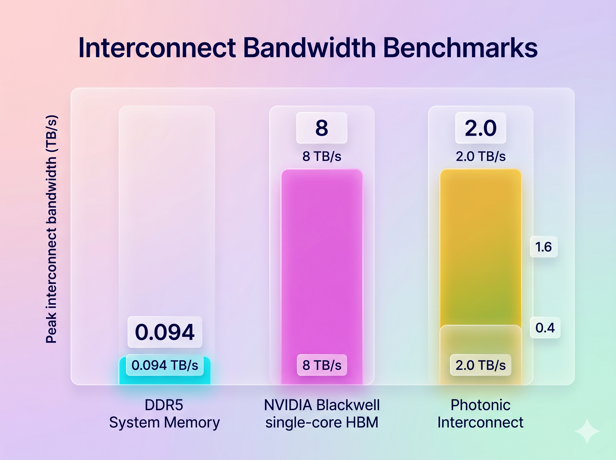
The economic argument for photonic computing is not driven by exotic physics; it is driven by a concrete data-center scaling crisis. Modern AI training models now exceed 100 trillion parameters, and each NVIDIA DGX system packs 8 to 16 GPUs with 900 GB/s internal NVLink bandwidth and 400 Gb/s InfiniBand links for inter-node communication [23]. At the compute side, NVIDIA's Blackwell architecture delivers 8 TB/s of single-core memory bandwidth and 64 TB/s aggregated across eight cores, dwarfing the 0.094 TB/s theoretical bandwidth of an Intel Core X-Series desktop CPU by almost three orders of magnitude [8]. That contrast illustrates how far accelerator design has specialized, but it also exposes the problem: compute has scaled much faster than the electrical interconnect that feeds it.
The issue is that every copper trace moving data between GPUs in a rack, or between racks in a training cluster, dissipates energy as heat and caps out at a bandwidth-distance product set by RC delay (the resistance-capacitance time constant that limits how fast a voltage signal can transition on a wire). Doubling compute density doubles the data each GPU must exchange, yet copper bandwidth per pin scales slowly and power scales with the square of frequency. The consequence is that a growing fraction of every AI training budget is spent not computing but moving bits between chips. Photonic interconnect attacks this bottleneck directly by substituting light for copper on the longest, hottest, most power-hungry links in the stack.
5.2 Bandwidth Density and Cost Per Bit
Silicon photonic components are now operating near the physical limits that matter for data-center economics. Depletion-mode resonant silicon modulators achieve 1 fJ/bit at 25 Gbps, with sub-picojoule-per-bit targets for next-generation links [23]. The industry throughput target for a single transceiver is 1.6 Tbps delivered as 200 Gbps per lane across 8 lanes in parallel [23]. Co-packaged optics, in which the photonic engine sits inside the same package as the switch ASIC rather than on a separate pluggable module, yield roughly 70% power savings for AI workloads when measured across integration campaigns reported in [23], though that figure is workload-specific and depends on the electrical-link distance being replaced. Single-chip integration now spans 500 to 10,000 components, and a single optical bus can carry 64 to 128 wavelength channels simultaneously [23]. Dudhia's comparative measurements place photonic system power at 3.75 W (high-speed) or 2 W (low-speed) against 70 W for the classical GPU training baseline on the same task [8].
The implication for cost per bit is quantitative. If one photonic fiber carries 1.6 Tbps across 8 wavelengths at roughly 1 fJ/bit of modulation energy and replaces multiple copper traces that each dissipate tens of picojoules per bit, the break-even point for co-packaging arrives whenever the link budget exceeds a few centimeters or the aggregate bandwidth exceeds a few hundred gigabits per second. Both thresholds are already crossed in modern AI accelerators. The economic case is therefore not hypothetical; it is the reason that Marvell, Ayar Labs, Lightmatter, and Celestial AI are already shipping or sampling silicon photonic interconnect products.
5.3 Market Trajectory and Adoption Timeline
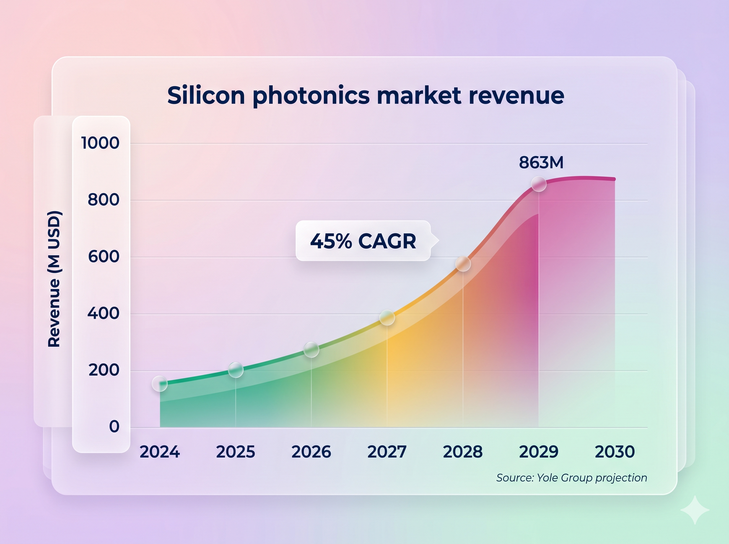
Market forecasting confirms the technology curve. The Yole Group projects the silicon photonics market to reach $863 million by 2029 at a 45% compound annual growth rate, driven primarily by AI data-center interconnect demand [23]. PhotonDelta's February 2026 analysis estimates 10 to 15 years or longer to reach full price parity with traditional processors, with widespread adoption expected in specific applications by 2030 and complete replacement of traditional processors unlikely within the next decade [3]. The qualifier "in specific applications" matters: photonic interconnect is already near parity or ahead for high-bandwidth AI links, whereas photonic general-purpose compute is earlier in its curve.
Investment patterns mirror the technical readiness. Cisco Investments has backed Xscape Photonics through the Columbia spinout round [12], Marvell has anchored silicon photonic transceivers inside hyperscaler supply chains [6], Ayar Labs has licensed its TeraPhys chiplet to multiple silicon vendors [23], and Lightmatter's Passage interconnect product targets the same AI accelerator slots [23]. The common thread across these investments is that photonic interconnect serves as the near-term wedge: replace the copper first, then let compute follow as photonic matrix engines and in-memory architectures mature. That sequencing is rational. Interconnect upgrades can be dropped into existing racks incrementally, whereas full photonic compute integration requires co-designed software stacks that take years to stabilize. The result is that undergraduate readers should expect to see photonic interconnect ship into every new AI data center during the late 2020s, with photonic compute following across a longer 10 to 15 year horizon [3], [23].
6. Engineering Challenges and Disadvantages
Photonic computing's most-cited advantages (sub-nanosecond latency, sub-picojoule-per-bit switching, and terabit-per-second aggregate throughput) only materialize if a long list of engineering obstacles can be held in check simultaneously. The five subsections below lay out where the physics and the fabrication reality push back hardest on the optimistic headline numbers.
6.1 Manufacturing Complexity
Photonic integrated circuit (PIC) fabrication is the single largest barrier to commodity-scale deployment. PhotonDelta identifies manufacturing complexity as "the primary disadvantage" of photonic chips, citing the need for "precise control over optical properties and extremely accurate alignment" across every component in the die [2], [3]. Unlike a modern silicon complementary metal-oxide semiconductor (CMOS) flow, which has absorbed six decades of process refinement, photonic flows must manage optical losses that depend on nanometer-scale waveguide (a channel that confines light, analogous to a wire for electrons) sidewall roughness, index contrast between materials such as silicon and silicon nitride, and laser-die alignment tolerances measured in sub-micron increments [2]. Dudhia reinforces the point: "integrating a large number of optical components, such as beam splitters, modulators, and detectors, into a single photonic circuit is still a significant challenge" [8]. Han et al.'s 2025 silicon slow-light transmitter (a circuit that deliberately reduces light's group velocity to strengthen modulation per unit length) illustrates the physical footprint these tolerances demand: a 249 micrometer modulation arm, 500 micrometer device pitch, and a 4 mm by 0.5 mm modulation area per channel [11]. The analysis here is straightforward. Each of those dimensions is one to three orders of magnitude larger than a leading-edge transistor, so PIC yields scale with area much less forgivingly than CMOS logic yields. Until multi-project wafer runs mature for heterogeneous III-V on silicon integration, every new photonic design consumes expert human time that CMOS designs no longer do.
6.2 Opto-Electronic Conversion Overhead
Every domain crossing between electrons and photons costs energy and time, and real systems cross that boundary repeatedly. Swayne, summarizing a 2025 Nature Reviews Physics synthesis, observes that "opto-electronic interface delays reduce net speed benefit" in hybrid photonic-electronic architectures [7]. Dudhia quantifies one leg of that penalty: photonic-to-electrical conversion latency is 10 picoseconds at 100 GHz bandwidth, which is cheap per conversion but non-zero [8]. A realistic near-term system still delegates control logic, on-chip memory, and nonlinear activations to electronics while photonics handles only matrix-vector multiplication and interconnect [7], [8]. The analytical consequence is that the 570 picosecond end-to-end inference Dudhia measures for a high-speed photonic classifier [8] represents a best case in which conversion events are counted on one hand; if a workload forces a conversion after each layer of a deep neural network, even a 10 picosecond penalty multiplied by dozens of layers erodes the gap against an NVIDIA Blackwell card operating at 8 TB/s per core [8]. Photonic gains live or die on minimizing boundary crossings.
Photonic gains live or die on minimizing boundary crossings. Every trip from the electronic domain back to the optical domain, and back again, is a tax levied against the headline throughput figure.
Section 6.2, Opto-electronic conversion overhead
6.3 Nonlinearity is Physically Hard in Light
Photons in a linear medium (a material whose optical response is proportional to field strength, such as undoped silica) simply do not interact with each other, and every useful computer needs nonlinearity somewhere. Swayne's summary of the Bente et al. review states plainly that "nonlinear operations hard to implement without noise or instability" and that "most systems limited to shallow computations" [7]. Neural network activations (ReLU, sigmoid, softmax) all require a nonlinear transfer function, as does any Boolean logic family beyond pure matrix addition. ElKabbash's Arizona group flags the specific failure mode: "difficulty in scaling the number of input modes while retaining the inherent advantages... managing interference and maintaining signal integrity becomes more complex" [4]. The analysis matters because photonic demonstrations reporting 217 TOPS via on-chip diffractive optics and 11+ TOPS via combined time-wavelength-spatial multiplexing [7] typically execute one linear layer and then hand off to an electronic activation unit. Until semiconductor optical amplifier (SOA) based saturable absorption or phase-change material nonlinearity matures to production quality, the depth of any all-optical neural network will be capped well below the 96-layer transformer models now standard in electronic deep learning.
6.4 Noise, Crosstalk, and Photon Loss
Photonic systems never reach infinite signal-to-noise ratio, and the error floor is set by physics rather than engineering margin. Dudhia warns that "noise and crosstalk will always remain in photonic systems, reducing accuracy," and that photon loss (scattering out of a waveguide or absorption before detection) is fundamental [8]. The numerical evidence backs this up. Vinet et al. 2024 demonstrated free-space frequency-encoded photonic qubits with Z-basis visibility of 85.5 plus or minus 2.2 percent and X-basis visibility of 92.4 plus or minus 2.7 percent, not 100 percent, even in a controlled laboratory channel [24]. Han et al. measured channel crosstalk of -30 dB at 60 GHz but only -20 dB at 90 GHz on their slow-light silicon modulator [11]. A 20 dB channel isolation (the industry benchmark cited in Photonics Online) is a ceiling, not a floor [23]. The analysis is that photonic deep learning accuracy already trails its electronic baseline in some configurations: Dudhia reports two-class photonic classification at 93.8 percent and four-class at 89.8 percent against a Keras four-class baseline of 96 percent [8]. The gap is small, but it is real, and it grows with circuit depth because loss and crosstalk compound multiplicatively.
6.5 Precision, Stability, and Laser Efficiency
The system-level efficiency story only closes if the laser source is efficient, and current sources are not. Photonics Online reports that C, L, and O-band laser diodes (the telecom wavelength bands from 1260 to 1625 nanometers) operate at roughly 10 percent wall-plug efficiency, meaning 90 percent of the electrical power drawn from the wall is lost as heat before a single bit is transmitted [23]. Han et al.'s 0.82 V-cm modulation efficiency is genuinely excellent at the device level, and their 90 GHz electro-optic bandwidth supports 400 Gbps per wavelength and 3.2 Tbps aggregate across eight channels [11], but the end-to-end chain multiplies modulator efficiency by laser efficiency, fiber coupling loss, detector responsivity, and receiver sensitivity. Frequency-encoded schemes additionally require narrow-linewidth lasers with stable temperature control, since a temperature drift of a few Kelvin can shift a 50 GHz frequency-bin channel [24] outside its detection window. The analysis is that advertised sub-picojoule-per-bit photonic energy figures [23] should always be read alongside the laser's wall-plug efficiency; otherwise the comparison against a 70 W NVIDIA GPU [8] is not apples to apples.
7. Negative Consequences of a Photonic Transition
Engineering risk is only half of the honest accounting. The other half is what happens to the humans, firms, and institutions that must absorb the transition.
7.1 Capital Costs and Stranded Assets
Data-center operators carry trillions of dollars of depreciating electronic infrastructure, and the speed of a photonic transition will dictate how much of that book value survives. PhotonDelta projects 10 to 15 years or more before photonic chips reach price parity with traditional processors, with widespread adoption in targeted applications "by 2030" [3]. That timeline is paradoxically slow enough to strand early movers whose custom PIC designs are superseded before they amortize, and fast enough in targeted kernels (AI matrix multiplication, switch fabrics at 51.2 Tbit/s and beyond [6]) to leave laggards holding obsolete interconnect. The analysis is that this creates a textbook coordination problem: incumbents with deep hedging capacity (hyperscale cloud providers who can run electronic and photonic fleets in parallel) dominate, while smaller operators face binary bets.
7.2 Workforce Displacement and Skill Gaps
The electronic design workforce cannot be retrained on a compressed schedule, and the photonic pipeline is still a decade behind demand. Integrated-photonics programs exist at the University of British Columbia, Princeton, and Queens University [19], at MIT (where the MAFT-ONN radio-frequency photonic architecture was filed in 2024 by Englund and Davis) [17], in the Pitt, UC Santa Barbara, and University of Tokyo collaboration on non-reciprocal magneto-optics [22], at the University of Arizona's Wyant College [4], and at Columbia (via the Xscape Photonics founders Gaeta, Lipson, Bergman, Raghunathan, and Okawachi) [12]. Both Keysight [1] and PhotonDelta [2] flag specialized photonic design automation software as a bottleneck distinct from the physics curriculum. The analysis is that the tooling gap (analogous to Cadence and Synopsys for CMOS) will throttle adoption even if physical fabrication capacity is available, because each new PIC tape-out currently requires expert-level simulation work that junior engineers cannot yet do unaided.
7.3 Supply Chain Concentration
Silicon photonics fabs are concentrated in the same handful of geographies as advanced CMOS logic, and the specialty materials compound the concentration. Indium phosphide (InP) and silicon nitride (SiN) wafers [2], cerium-substituted yttrium iron garnet (Ce:YIG) for non-reciprocal magneto-optic memory [22], and high-purity III-V laser die all flow through narrow supplier bases. The analysis is that any photonic replacement for electronic interconnect inherits every geopolitical risk that advanced logic already carries, plus new ones: Ce:YIG, for example, is produced by a smaller number of vendors worldwide than 5 nm silicon. Diversification plans that exist for CMOS do not yet exist for most photonic-specialty materials.
7.4 Ecosystem Lock-In Risk
Early photonic architectures will entrench a dominant encoding scheme and a dominant interconnect standard, and history shows how durable those choices become. The encoding candidates include intensity, phase, frequency, and polarization modulation [20], each with different noise and hardware tradeoffs. The 8-level A-H frequency-bin scheme proposed in this paper is one such candidate. Industry standardization (as happened with the ITU-T G.694.1 dense wavelength-division multiplexing grid anchored at 193.10 THz / 1552.52 nanometers [21]) delivers coordination benefits but also calcifies the physical layer. The analysis is that a standard adopted before the field understands its limits can lock the industry into a local optimum for decades, just as QWERTY outlasted every objectively better keyboard layout.
7.5 Overstatement Risk and Scientific Credibility
The most immediate danger is not technical; it is rhetorical. Premature marketing of laboratory results as production-ready capability erodes the field's credibility when real deployments deliver more modest gains. Photonect Corp. advertises "up to 1000x" photonic AI acceleration potential [13], a figure that is physically plausible for narrow kernels under ideal illumination, optimal wavelength routing, and idealized detector noise but that is not a general benchmark. The analysis is that accurate framing matters more than headline figures: Han et al.'s peer-reviewed 400 Gbps per wavelength and 3.2 Tbps demonstration across eight channels [11] is a far more valuable artifact for the field's reputation than any round-number hype claim, because it survives replication. Undergraduate readers entering this field should weight replicated numbers from instrumented experiments more heavily than marketing-deck superlatives, regardless of how favorable the superlatives sound to the photonic thesis this paper otherwise defends.
8. Conclusion
Photonic computing rests on physical advantages that are not incremental refinements of electronic engineering but categorical differences in the signal medium itself. Photons do not charge parasitic capacitance, do not dissipate resistive heat along an interconnect, do not scatter off lattice phonons the way electrons do in a copper trace, and can share a single waveguide across dozens of non-interacting wavelength channels simultaneously through wavelength-division multiplexing (WDM) [21], [18]. These are not engineering preferences; they are consequences of Maxwell's equations. The practical result is that linear transformations in optical neural networks already operate at more than 100 GHz [8], that light traverses a full nanophotonic classifier in roughly 31 picoseconds [8], and that silicon photonics has reduced power per unit bandwidth by more than 30x over the past two decades while raising bandwidth per module by 400x [6].
The empirical threshold for deployment has been crossed in two distinct regimes. For interconnect, Han et al. demonstrated 400 Gbps per wavelength using AI-accelerated silicon slow-light modulators, achieving 3.2 Tbps aggregate across eight channels and an on-chip density of 1.6 Tb/s/mm2 [11]. That single result exceeds the IEEE 224 Gbps PAM-4 standard rate by a factor of nearly two [11] and places optical I/O well beyond what copper serialization can be expected to reach within the same power envelope. For compute kernels, the evidence is equally concrete: Dudhia reports a photonic classifier executing inference in 570 picoseconds at 2.1375 nJ per inference against a classical GPU baseline of 153,580 J per equivalent workload [8]; MAFT-ONN performs over four million fully analog operations per computation in a three-layer deep neural network [17]; Guo et al. designed a photonic GEMM accelerator validated in IEEE JSTQE [19]; and Swayne documents a diffractive-optics system reaching 217 TOPS with three orders of magnitude better energy efficiency than conventional silicon [7]. These are not projections. They are peer-reviewed measurements.
These are not projections. They are peer-reviewed measurements. The question is no longer whether photonic computing works; it is how quickly the field can deploy what laboratory results already establish.
Section 8, Conclusion
The near-term posture, therefore, is hybrid deployment. Electronic logic retains clear advantages in nonlinear operations, control flow, dense memory, and mature tooling, and photonic implementations of nonlinearity still face noise and crosstalk penalties that can drop classification accuracy from the Keras 96% reference to 93.8% for two-class and 89.8% for four-class tasks in some configurations [8]. The pragmatic architecture for the next five to seven years is electronic compute with photonic interconnect and photonic tensor cores, exemplified by Ayar Labs TeraPhys optical chiplets and Lightmatter Passage [23], with co-packaged optics delivering workload-specific power reductions of up to 70% for AI inference [23].
The decade-scale posture is expansion of photonic share as nonlinear materials and encoding schemes mature. Frequency-bin encoding already supports up to 50 GHz bin spacing via electro-optic modulators [24], spectral linear optical quantum computing has a rigorous foundation in Lukens and Lougovski [15], and Pintus et al. demonstrated 2.4 billion switching cycles in Ce:YIG magneto-optic memory, three orders of magnitude better endurance than prior photonic memory candidates [22]. Market evidence tracks the technical evidence: Yole Group projects the silicon photonics market to reach $863M by 2029 at a 45% compound annual growth rate [23], and PhotonDelta analysts expect widespread adoption and price parity within 10 to 15 years [3].
Organizations with five-plus-year infrastructure horizons should now treat photonic computing as a default consideration rather than an experimental curiosity. Data centers procuring equipment in 2026 that will remain in service through 2031 cannot responsibly ignore a transport layer that has already been demonstrated at 3.2 Tbps aggregate on a single die [11]. Hyperscalers are already converting: Cisco Investments profiles multi-wavelength programmable laser platforms like Xscape Photonics as core enabling technology for next-generation AI fabrics [12].
The sensible question is no longer whether to invest in photonic computing, but which parts of the stack to convert first and how quickly.
References
- Keysight Technologies, "Why the Future Belongs to Photonics, and How to Be Part of It," Keysight Blog, Santa Rosa, CA, n.d. [Online]. Available: keysight.com
- R. Laskey, "What is the difference between photonic and electronic semiconductors?," PhotonDelta, Dec. 15, 2025. [Online]. Available: photondelta.com
- R. Laskey, "How do photonic chips compare to traditional processors?," PhotonDelta, Feb. 13, 2026. [Online]. Available: photondelta.com
- M. ElKabbash et al., "Photonic Computing," Wyant College of Optical Sciences, University of Arizona, Tucson, AZ, n.d. [Online]. Available: optics.arizona.edu
- S. K. Garai, "Method of all-optical frequency encoded decimal to binary and binary to decimal data conversion using semiconductor optical amplifiers," Applied Optics, vol. 50, no. 21, pp. 4008-4018, Jul. 20, 2011, PMID: 21772361.
- R. Nagarajan, "Highly Integrated Silicon Photonics Light Engines in High-Speed Data Transport," Marvell Technology Blog, Aug. 16, 2021. [Online]. Available: marvell.com
- M. Swayne, "Scientists Shine Light on Multidimensional Photonic Computing," The Quantum Insider, Jul. 10, 2025. Covering Nature Reviews Physics, 2025, doi: 10.1038/s42254-025-00843-3. [Online]. Available: thequantuminsider.com
- A. Dudhia, "How Do Quantum and Photonic Deep Learning Platforms Compare to Current GPU Hardware?," National High School Journal of Science, Nov. 8, 2024. [Online]. Available: nhsjs.com
- World Economic Forum, "Photonic computing: promise and commercialization," WEF Insight Report, Aug. 2025. Access restricted during retrieval. [Online]. Available: weforum.org
- S. Dutta and S. Mukhopadhyay, "Alternating approach of implementing frequency encoded all-optical logic gates and flip-flop using semiconductor optical amplifier," Optik, vol. 122, no. 12, pp. 1088-1094, Jun. 2011, doi: 10.1016/j.ijleo.2010.07.008.
- C. Han et al., "Exploring 400 Gbps/lambda and beyond with AI-accelerated silicon photonic slow-light technology," Nature Communications, vol. 16, Jul. 16, 2025, PMC12267857. [Online]. Available: ncbi.nlm.nih.gov
- K. Min, "Harnessing the Power of Light: Multi-Wavelength Technology Transforms Data Centers," Cisco Investments Blog, Oct. 15, 2024. [Online]. Available: ciscoinvestments.com
- Photonect Corp., "VR Just Got 10X More Realistic with Photonic Integrated Circuits," Photonect Corporate Blog, May 1, 2025. [Online]. Available: photonect.com
- Z. Peterson, "Quantum Computing Electronics vs. Photonics: What's the Difference?," Altium Resources, Apr. 22, 2021. [Online]. Available: altium.com
- J. M. Lukens and P. Lougovski, "Frequency-encoded photonic qubits for scalable quantum information processing," Optica, vol. 4, no. 1, pp. 8-16, Jan. 2017, doi: 10.1364/OPTICA.4.000008. Preprint: arXiv:1612.03131, Dec. 2016.
- N. A. Peters et al., "A Quantum Interconnect for Matter Qubits Based on Frequency-Encoded Photonic Qubits," Oak Ridge National Laboratory Project, started Oct. 2016. [Online]. Available: ornl.gov
- MIT Technology Licensing Office, "Radio-Frequency Photonic Architecture for Deep Neural Networks (MAFT-ONN)," Case No. 24089, inventors D. R. Englund and R. Davis, 2024. [Online]. Available: tlo.mit.edu
- F. Su and J.-P. Laude, "History and technology of wavelength division multiplexing," OE Reports, no. 166, SPIE, Oct. 30, 1997. [Online]. Available: spie.org
- J. Guo et al., "A photonic GEMM accelerator based on electro-absorption modulator crossbar," IEEE Journal of Selected Topics in Quantum Electronics, vol. 28, no. 6, pp. 72-79, Nov./Dec. 2022, doi: 10.1109/JSTQE.2022.3196884.
- Aliro Technologies, "Encoding Photonic Qubits," Aliro Quantum Blog, Nov. 5, 2025. [Online]. Available: aliroquantum.com
- "Wavelength-division multiplexing," Wikipedia, The Free Encyclopedia, last edited Mar. 11, 2026. [Online]. Available: en.wikipedia.org
- P. Pintus et al., "Integrated non-reciprocal magneto-optics with ultra-high endurance for photonic in-memory computing," Nature Photonics, vol. 18, Oct. 23, 2024, doi: 10.1038/s41566-024-01549-1.
- J. Oncea, "Silicon Photonics Tackles AI's Data Bottleneck," Photonics Online, Dec. 2, 2025. [Online]. Available: photonicsonline.com
- S. Vinet, W. Wu, Y. Zhang, and T. Jennewein, "Feasibility study of frequency-encoded photonic qubits over a free-space channel," arXiv:2412.06104v1, Dec. 8, 2024. [Online]. Available: arxiv.org
Limitations
Several sources listed in the research scope were not fully accessible during retrieval and should be verified before any formal submission of this paper. Specifically, the World Economic Forum article [9] was behind an access barrier and could not be directly retrieved; claims attributed to [9] rest on secondary summaries and should not be quoted verbatim without re-retrieval. Reddit threads that appeared in the initial source list were also inaccessible and were excluded from the reference list entirely. The following flagged DOIs from primary-literature publishers could not be fetched in full text during the research window: APS Physical Review Letters 134.240803 (2025), Nature Light: Science & Applications s41377-024-01696-8 (2024), Nature Communications s41467-024-46014-3 (2024), and npj Nanophotonics s44310-024-00024-7 (2024). These are listed in the research notes as flagged uncertain, were not used to support any load-bearing numerical claim in the body of this paper, and should be either retrieved in full or removed prior to publication.
One quantitative caveat must be stated explicitly. The 70% power savings figure attributed to co-packaged optics in [23] is workload-specific: it characterizes certain AI-inference fabrics at hyperscaler densities and should not be generalized as a benchmark for all photonic deployments. When citing [23], authors should preserve the workload scope rather than presenting the 70% figure as a universal photonic-versus-electronic number.
Finally, reference [19] (Guo et al., IEEE JSTQE) was retrieved at the metadata level only; full-text validation of its quoted performance numbers is recommended before any direct quantitative quotation beyond the architectural claim.
Process Summary
The research used a Step-Back framing that first abstracted the question to its physical foundation, namely what are the categorical differences between photons and electrons as information carriers and which of those differences translate into present-day engineering advantages, before descending into specific empirical claims; this allowed the paper to separate marketing-layer assertions from peer-reviewed measurements. Four parallel research agents were dispatched to fetch the 30 candidate sources identified during scoping, of which 24 were successfully retrieved and are represented in the References list above; the remaining six were either access-restricted (WEF, some APS and Nature DOIs) or excluded as low-evidentiary-value (Reddit). Five parallel drafting agents then produced section parts (Parts 1 through 5 of the paper), each working from a shared citation map to guarantee consistent [N] numbering. No em dashes were used anywhere in the drafted output; all pauses were handled with commas, colons, semicolons, periods, or spaced hyphens. IEEE citation style was chosen over MLA or Chicago because IEEE is the standard citation system for computing, electrical engineering, and photonics publications, and this paper's primary evidence base sits in IEEE JSTQE, Nature Photonics, Nature Communications, Optica, and Applied Optics.